Zap++ - An EMS System for Fine-Grained Wearable Force Feedback
| Leitung: | Tim Dünte |
| Team: | Tim Dünte, Max Pfeiffer, Michael Rohs |
| Jahr: | 2017 |
| Ist abgeschlossen: | ja |
| Weitere Informationen | https://www2.hci.uni-hannover.de/research/zap++/ |
Zap++
A 20-Channel EMS System for Fine-Grained Wearable Force Feedback
Electrical muscle stimulation (EMS) has been used successfully in HCI to generate force feedback and simple movements both in stationary and mobile settings. However, many natural limb movements require the coordinated actuation of multiple muscles. Off-the-shelf EMS devices are typically limited in their ability to generate fine-grained movements, because they only have a low number of channels and do not provide full control over the EMS parameters. More capable medical devices are not designed for mobile use or still have a lower number of channels and less control than is desirable for HCI research. We present the concept and a prototype of a 20-channel mobile EMS system that offers full control over the EMS parameters. We discuss the requirements of wearable multi-electrode EMS systems and present the design and technical evaluation of our prototype.
On this page we offer technical details, as schematics, PCB layouts and additional pictures of the prototype. For more information refer to our paper: Zap++: A 20-Channel EMS System for Fine-Grained Wearable Force Feedback
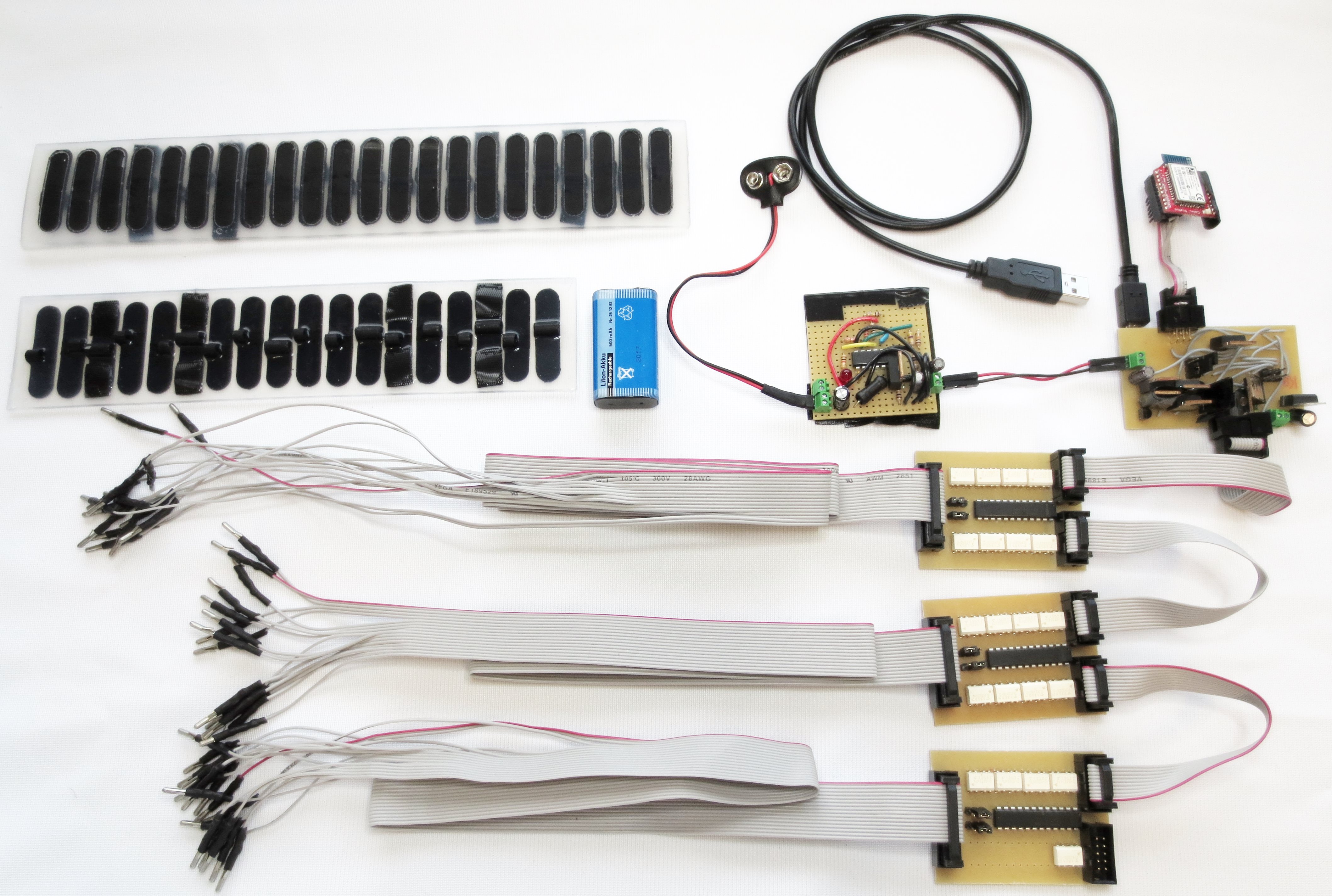
Components
Zap++ is a prototype to generate fine-grained EMS feedback in mobile context. It consists of the following components:
- signal generation board
- switching boards
- electrode sleeves
- power source
The components are exchangeable. Different grids with different layouts can be connected to the switching boards. Additional switching boards or different kind of switching boards could be connected to the signal generation circuit. The Signal generation unit or the grids connected to the switching boards could be either used seperate as single components.
Signal Generation Board
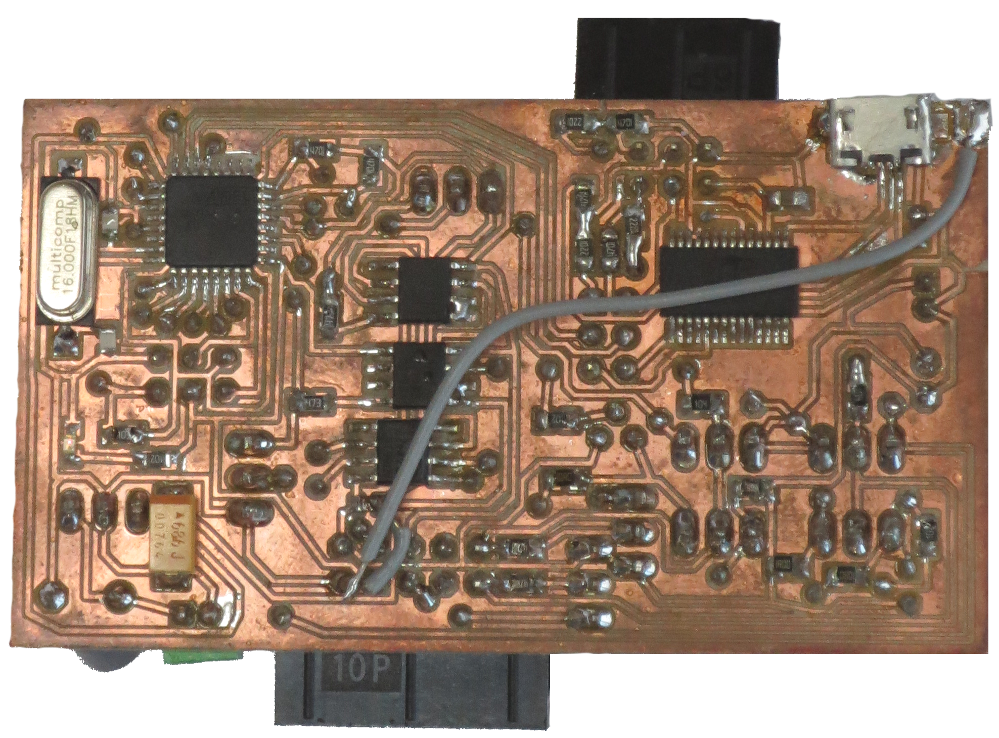
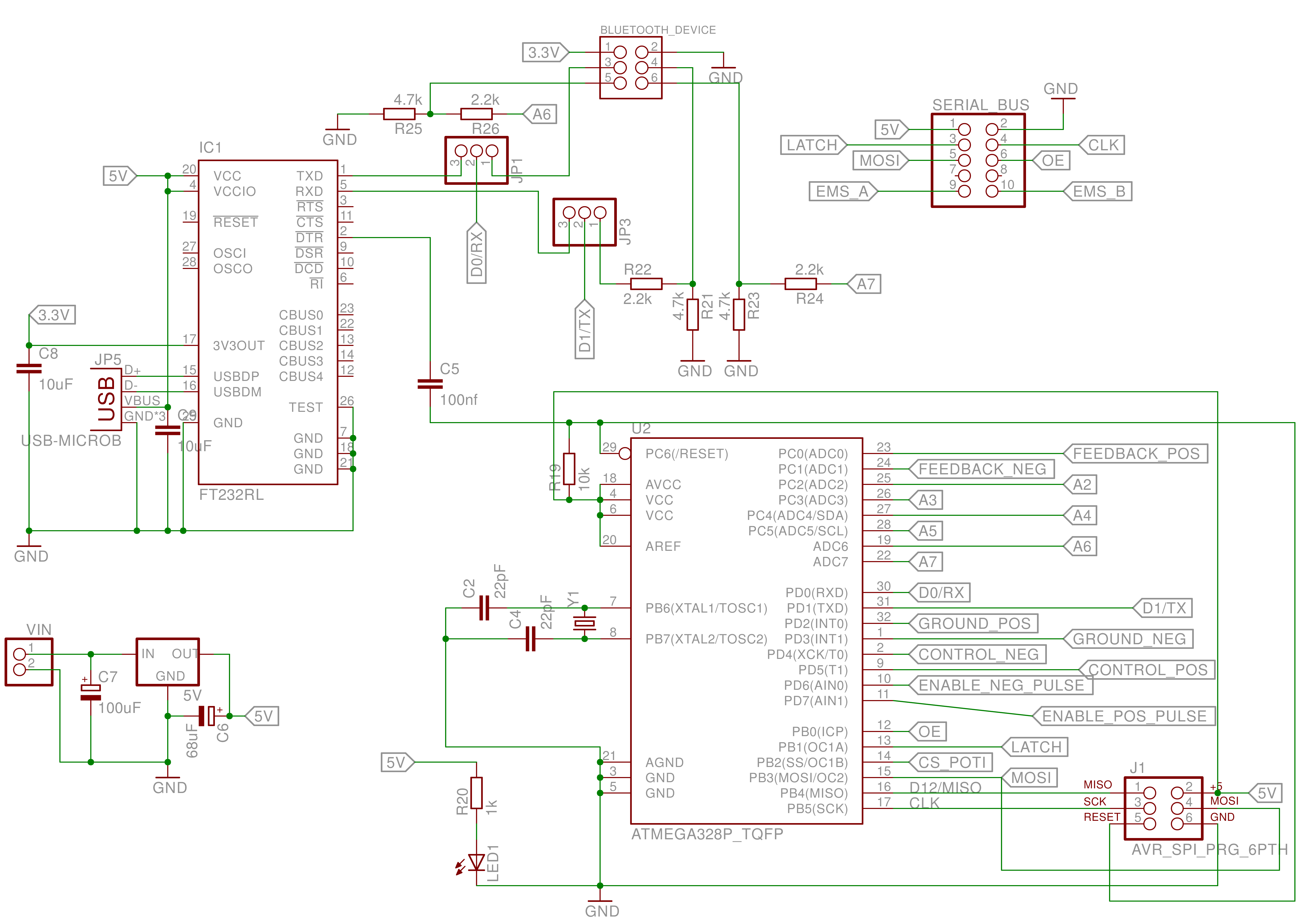
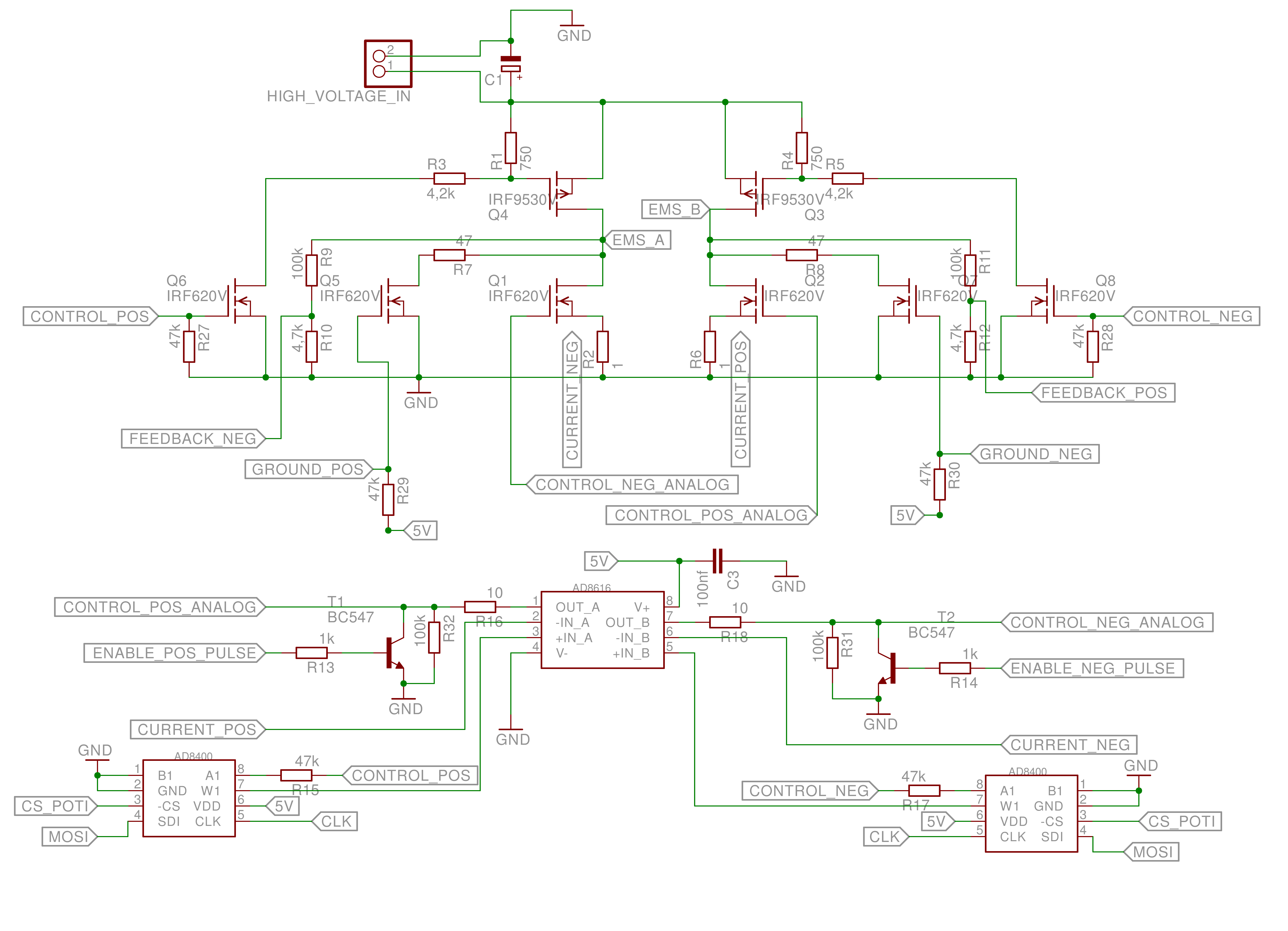
Schematics
These are pictures of the schematics of the signal generation board. The left picture shows the control and communication part including the Bluetooth connection and the serial interface for the switching boards. The right schematics shows the H-bridge and current regulation part.
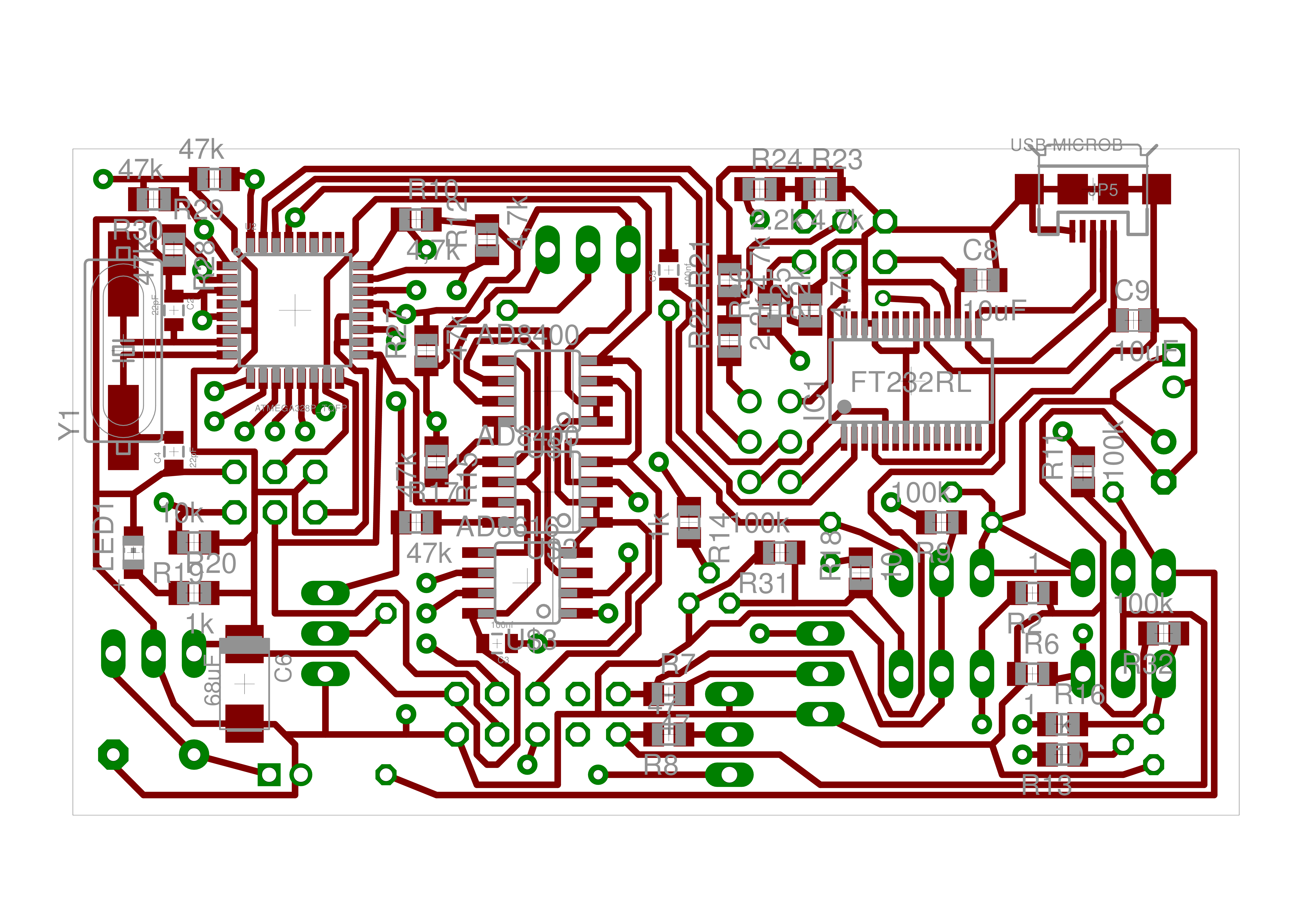
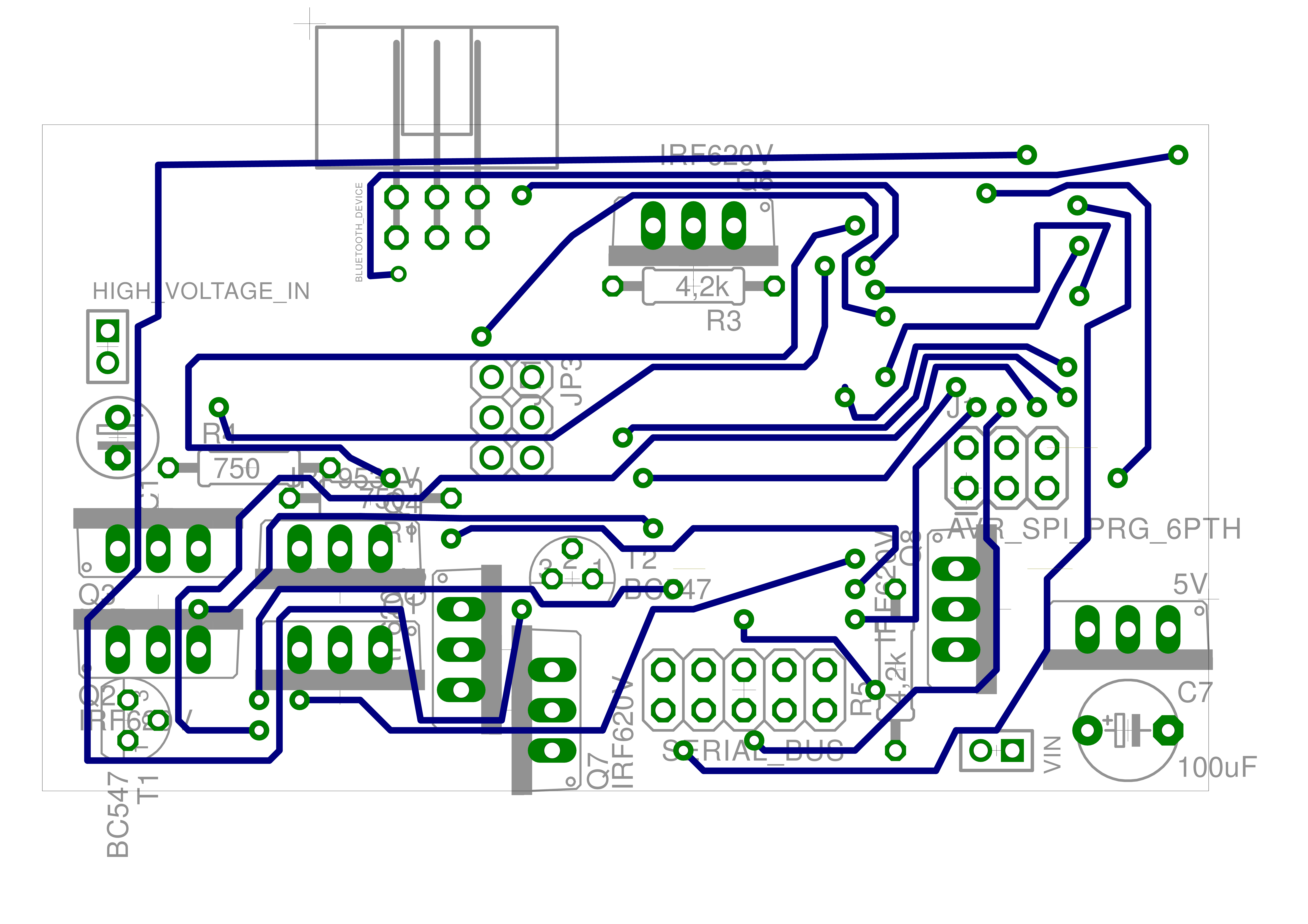
Layout
The layout of the board is designed as two sided PCB. But it is also possible to use a single sided PCB. The blue wires in the right figure have to be connected manually.
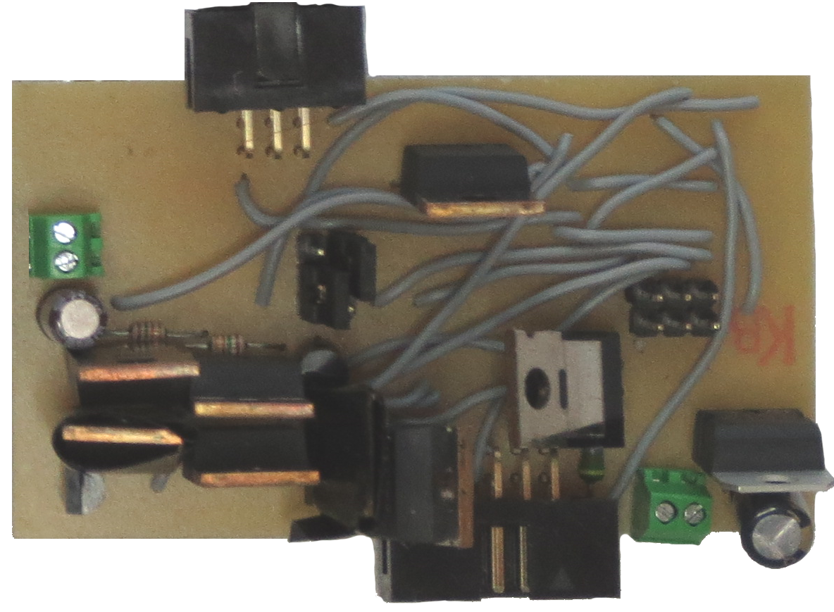
Switching Board
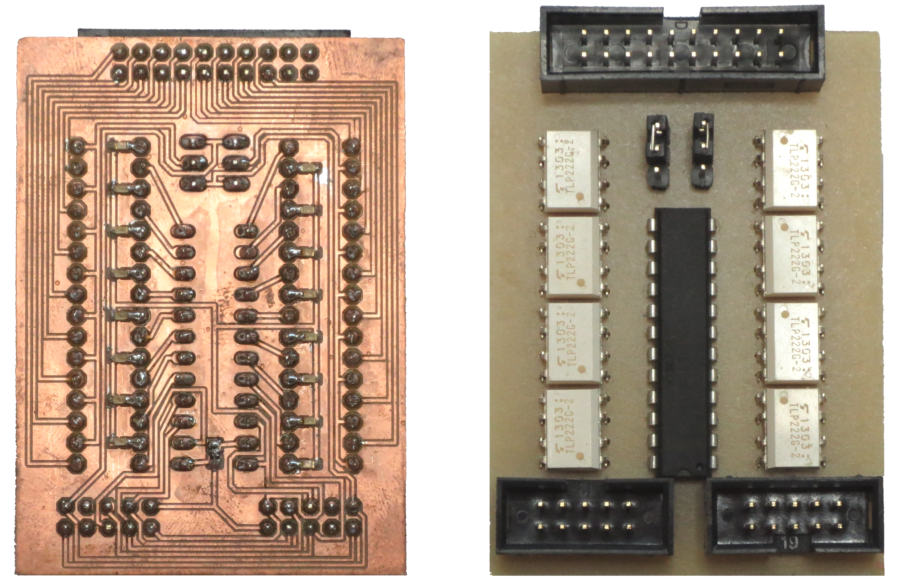
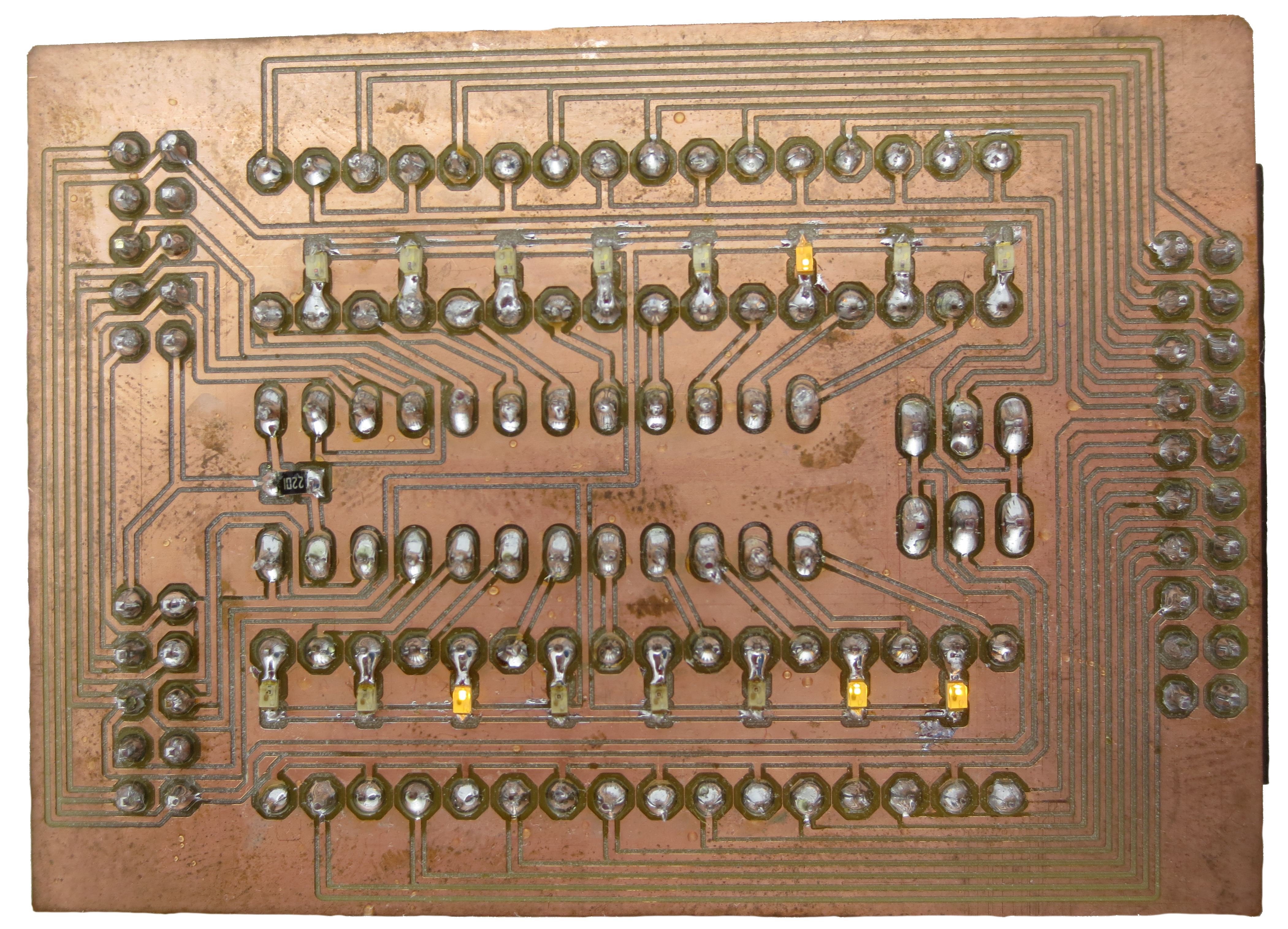
The switching board consists of a LED driver IC (MAX6969), LEDs for debug purposes and photo MOS relays. A LED glows if the connected relay is activated. The remaining space on the board is used for signal routing. Jumper on the center of the board enable the configuration of 8 electrodes. A group of eight electrodes could be connectred either to clamp A or B on
Schematics
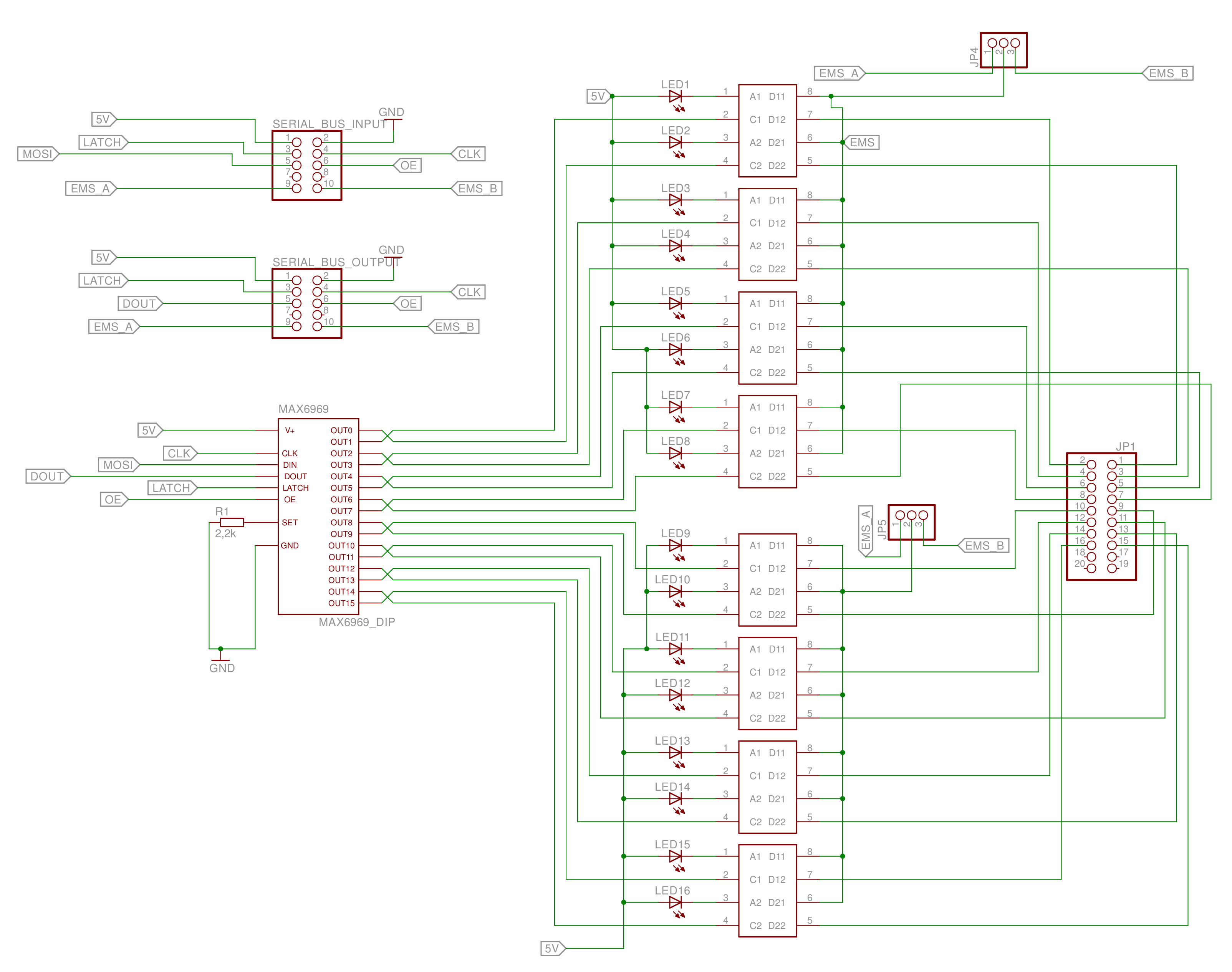
The switching boards are connected serialy. It is possible to connect multiple switching boards in row. Except of one signal all signals are routed directly from the input header to the output header. Only the data signal is routed through the MAX6969.
Layout
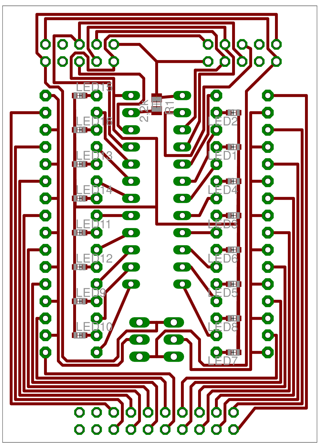
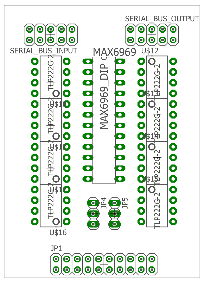
The switching boards are single sided. As this is a first prototype we used through hole components instead of SMD components.
Additional Material
Electrode Sleeves
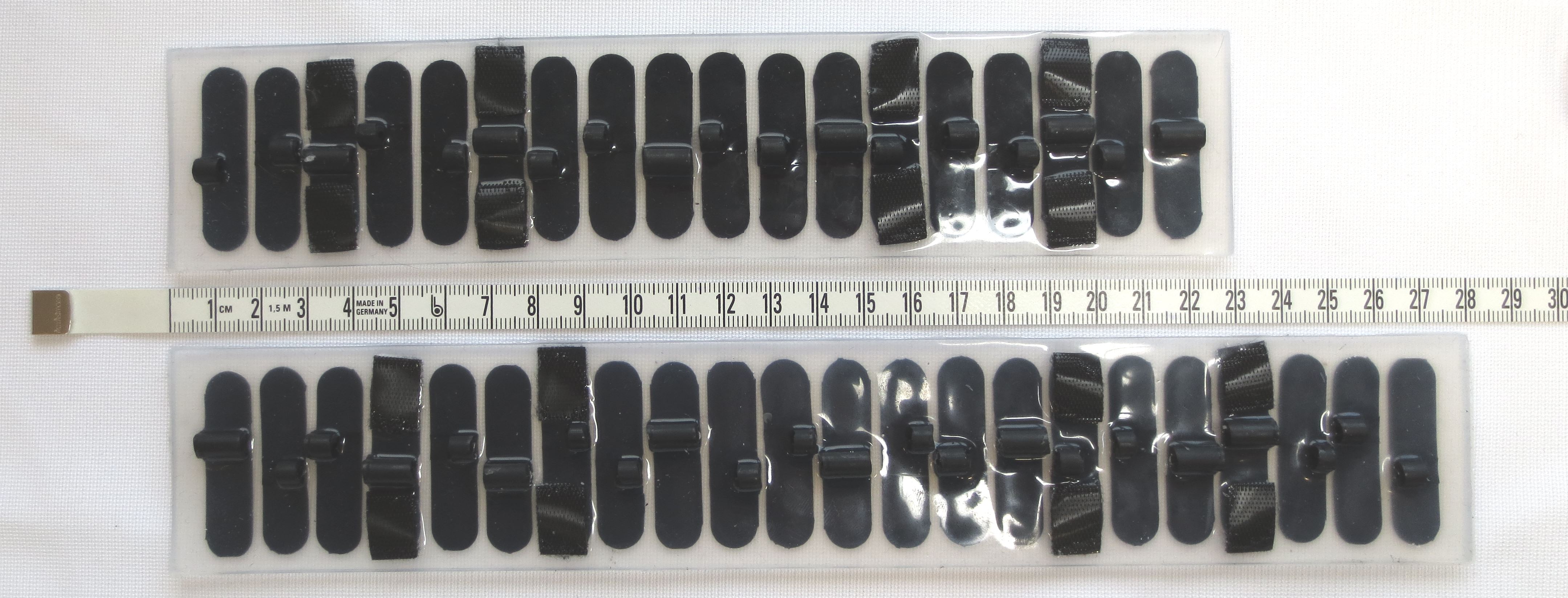
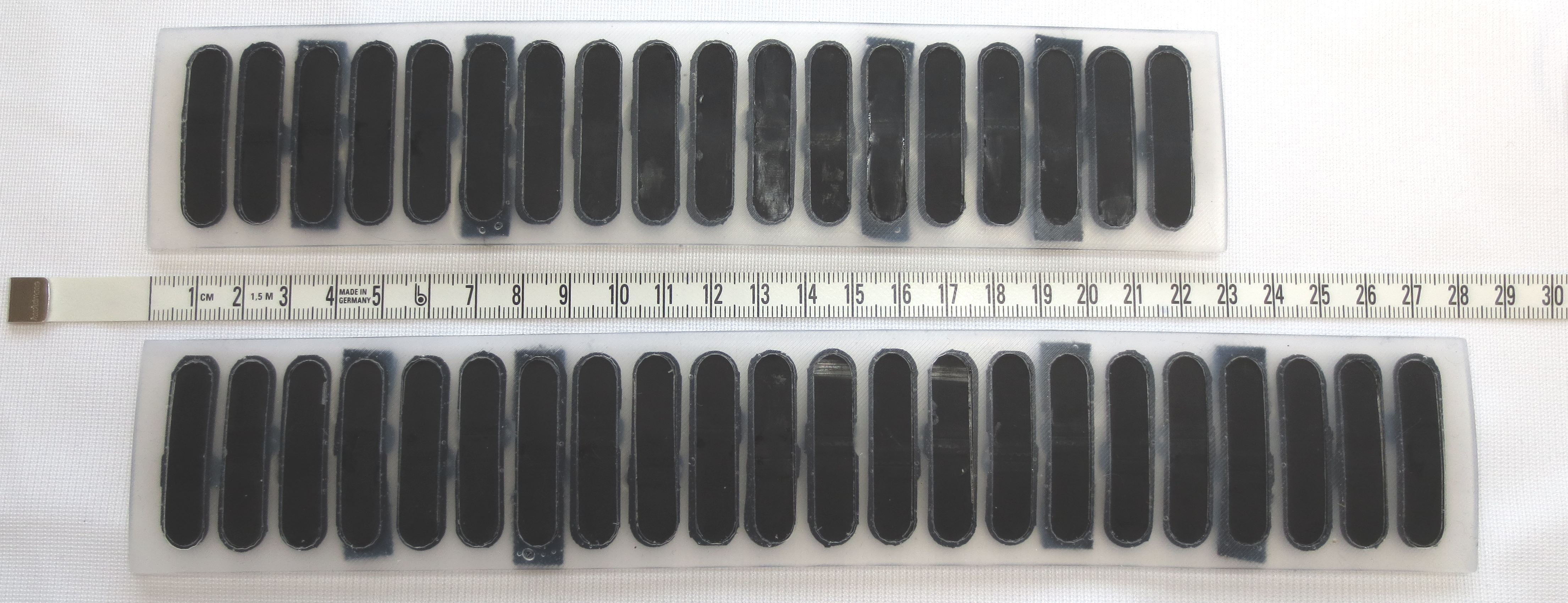
The electrodes we used were carbon rubber electrodes. These were cut into smaller pieces and then molded in silicon. The pictures below show the produced sleeves and the form, that we created with a 3D Printer.
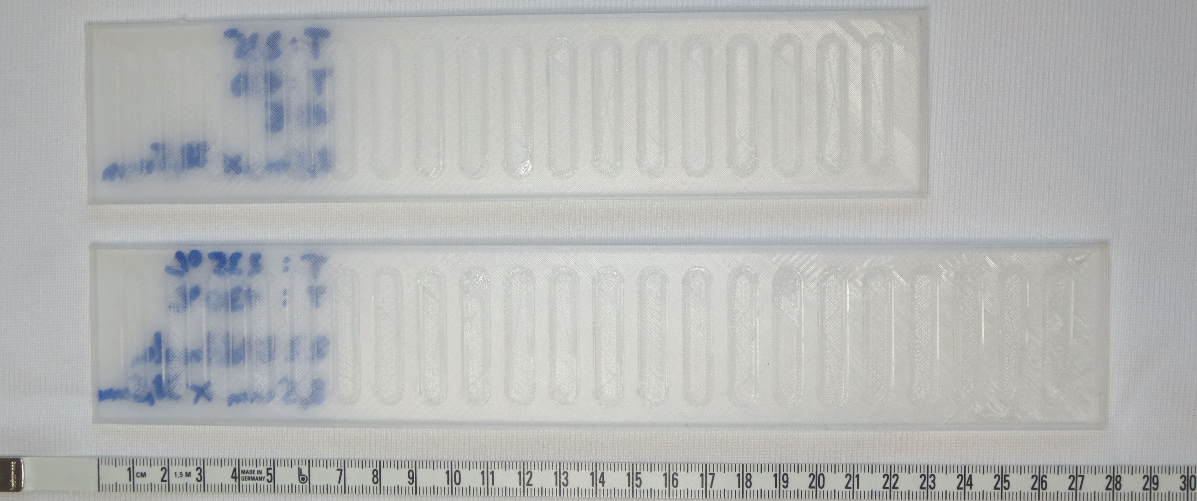
Additional Material
The design of the electrode form was done in OpenSCAD.
Testing the Prototype
Video
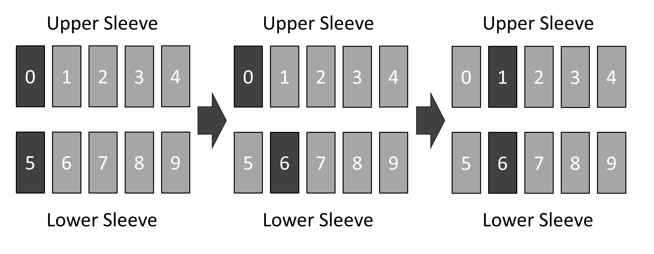
The video shows a calibration of the system with the Zap++ prototype. On the left there is the weared Zap++ prototype on the forearm of a user. On the right there is a calibration application, that activates electrode pairs and increases the EMS intensity. The intensity per electrode pair is increased until the intensity is felt as uncomfortable. This calibration approach is intended to get an intensity profile of the forearm. Therefore not all in the paper described electrodes pair combinations are tested (see picture below for tested combinations). This approach takes typically 8 minutes. A calibration with all tested pairs needs about 18 minutes
Calibration
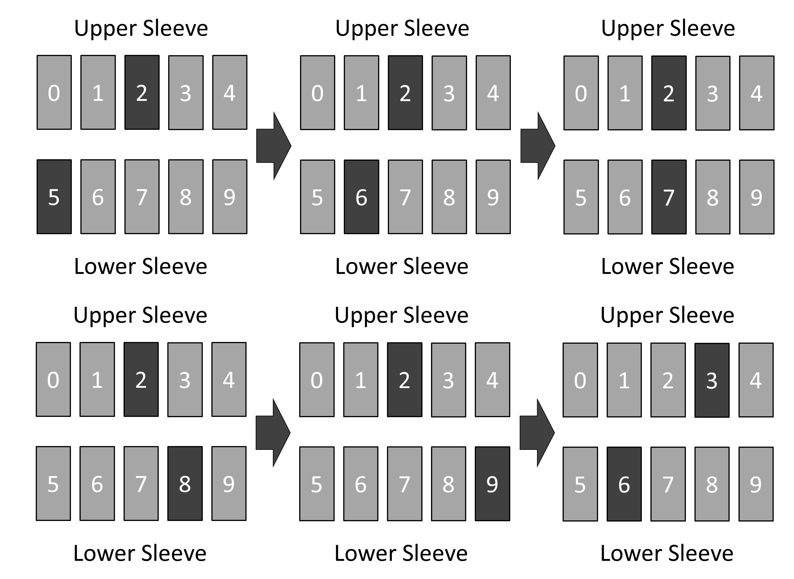
For a calibration to control single muscle movements of the hand we tested more electrode pairs. Each electrode of the upper sleeve was tested with five electrodes of the lower sleeve as described in the paper to control as many muscles as possible.
Zap++ - Version 2
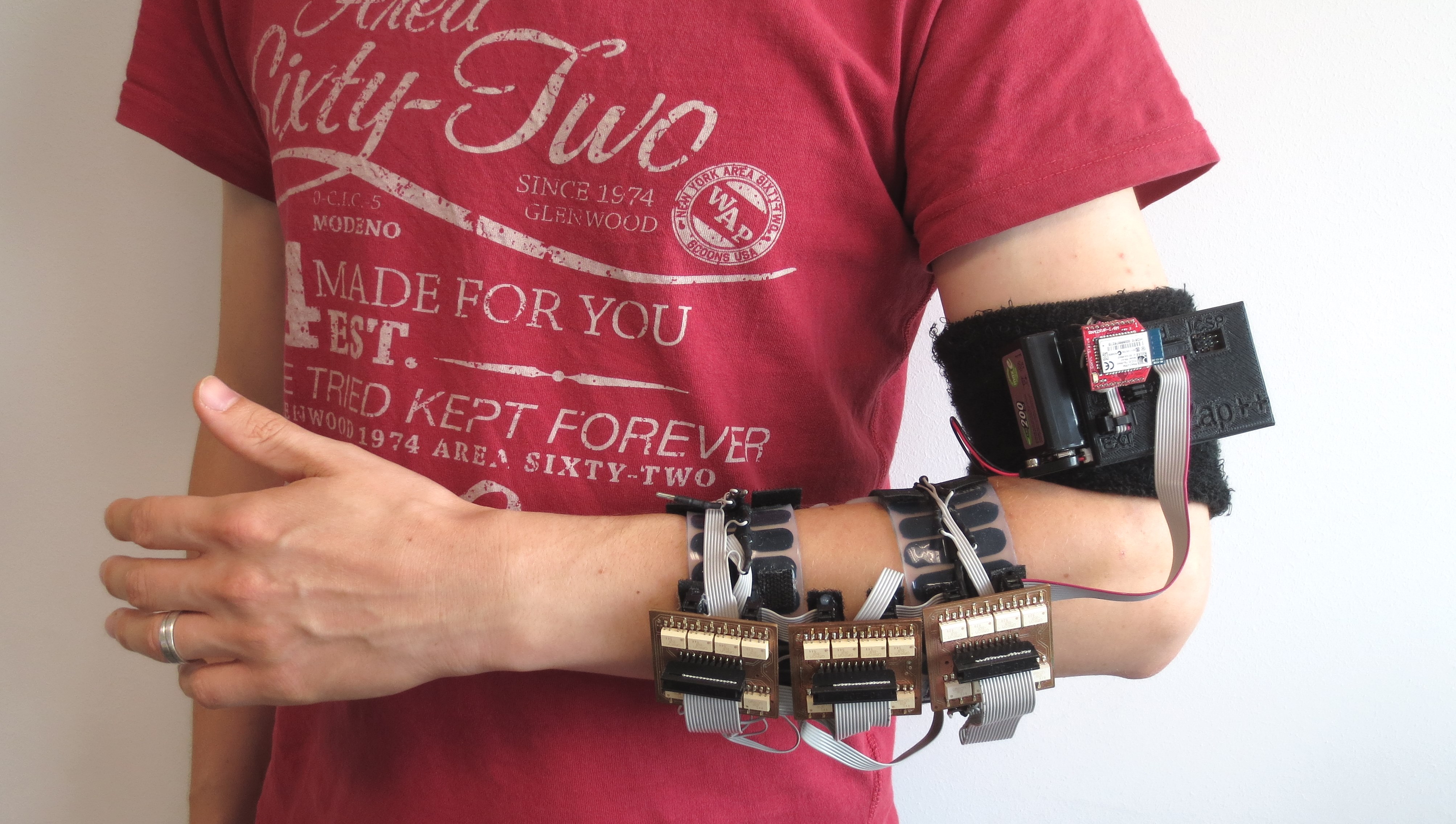
As mentioned in the paper we worked on mobility of the prototype and created a version, that uses SMD parts. In contrast to the first version the prototype is smaller and consumes less power. Also the cables are shorter and the prototype is fully wearable on the arm. The signal generation and control unit is protected by a casing.


